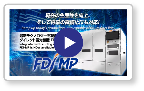
Video
Video
Repeat product videos for related systems
FDi-MP
FDi-MP
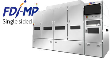
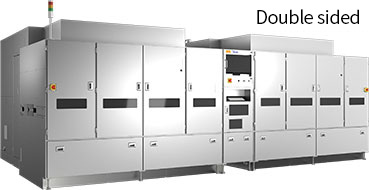
Applications: Patterning for high-resolution package PCB
- FC-BGA Substrates
- FC-CSP substrates
- Various module substrates such as AiP
Features
- -Direct exposure of circuit patterns of 10 µm or less
- -ORC's unique alignment compensation technology enables high-precision pattern alignment
- -The ability to switch between productivity-oriented and resolution-oriented exposure modes allows for product development and mass production with a focus on current and future mass production.
- -Expanded lineup of application-specific products based on FDi-MP
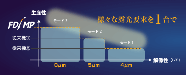
Product specification
Product specification
| Item | Mode 1 | Mode 2 | Mode 3 |
|---|---|---|---|
| Light source | Semiconductor laser | ||
| Resolution(L/S) | 4 μm | 5 μm | 8 μm |
| Data resolution | 0.1 / 0.25 / 0.5 μm | ||
| Maximum exposure size | 515 x 515 mm | ||
| Total Overlay Accuracy | 3.5 μm | ||
Exposure Mode
Exposure Mode
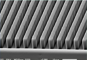
3μm L/S (Mode 1 applied)
FDi-Ms
FDi-Ms
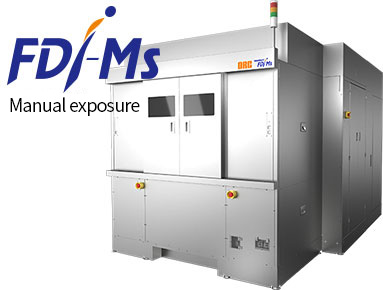
Applications:
- -Material development
- -Glass mask imaging, etc.
Features:
- Optical head configurations can be proposed according to your budget
FDi-MPW
FDi-MPW
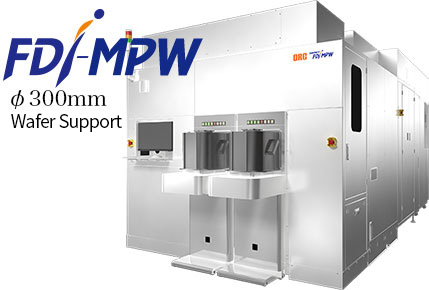
Applications:
- FO-WLP via formation, RDL formation
Features:
- Die by Die alignment function is available.
Exposure corresponding to die shift is possible with a system by it self.
RDi-MP Duo
RDi-MP Duo
Applications:
- Pattern exposure for COF and high-resolution FPC
Features:
- Improved productivity by simultaneous transport and exposure of two rolls of material